��
|
2011 and after
2010 and before |
|
YEAR 2010 |
|
 |
��
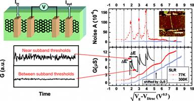
Xu, G.; Torres, C.M.; Song, EB.; Tang, J.; Bai, J.; Duan,
X.; Zhang, Y. and Wang K.L. (2010). Enhanced conductance
fluctuation by quantum confinement effect in graphene
nanoribbons, Nano Lett. 10,
4590�C4594
(doi:
10.1021/nl1025979).
�� |
|
 |
��
Qu, Y. and Duan X. (2010). Highly efficient photocatalysts from nanoscale metal/semiconductor/metal
heterojunctions, ECS Trans. 33(9),
23-38. (e-link)
�� |
|
 |
��
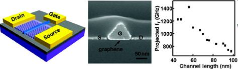
Liao, L.; Bai, J.; Cheng, R.; Lin, Y.; Jiang, S.; Qu, Y.;
Huang, Y. and Duan, X. (2010). Sub-100 nm channel
length graphene transistors, Nano Lett. 10,
3952-3956 (doi: 10.1021/nl101724k).
�� |
|
 |
��
Lopata, K.; Thorpe, R.; Pistinner, S.; Duan, X.
and Neuhauser, D. (2010). Graphene nanomeshes: onset of conduction
band gaps, Chem. Phys. Lett.
498,
334-337
(doi:
10.1016/j.cplett.2010.08.086).

�� |
|
 |
��
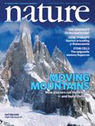
Liao, L.; Lin, Y. C.; Bao, M. Q.; Cheng, R.; Bai, J. W.;
Liu, Y.; Qu, Y. Q.; Wang, K. L.; Huang, Y.; and Duan, X.
(2010). High speed graphene transistors with a self-aligned
nanowire gate, Nature. 467, 305 (doi:
10.1038/nature09405).
�� |
|
 |
��
Xu, G.; Bai, J.; Torres, C.M.; Song, E.B.; Tang, J.; Zhou,
Y.; Duan, X.; Zhang, Y. and Wang, K. (2010).
Low-noise submicron channel graphene nanoribbons, Appl.
Phys. Lett. 97, 073107 (doi: 10.1063/1.3481351).
�� |
|
 |
��
Bai., J.; Cheng, R.; Xiu, F.; Liao, L.; Wang, M.; Shailos,
A.; Wang, K.; Huang., Y. and Duan, X. (2010). Very
large magnetoresistance in graphene nanoribbons, Nature
Nanotech. 5, 655-659 (doi: 10.1038/nnano.2010.154).
�� |
|
 |
��
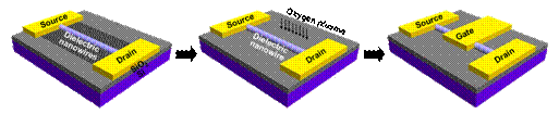
Liao, L.; Duan, X. Graphene�Cdielectric integration for
graphene transistors (2010). Materials Science and
Engineering: R: Reports 70, 354-370 (doi: 10.1016/j.mser.2010.07.003).
�� |
|
 |
��
Freer, E.; Grachev, O.; Duan, X.; Martin, S. and Stumbo, D. (2010). High-yield self-limiting single-nanowire
assembly with dielectrophoresis, Nature Nanotech. 5,
525-530 (doi: 10.1038/nnano.2010.157).
�� |
|
 |
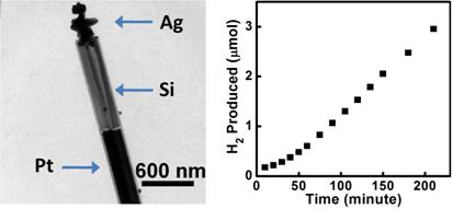
��
Qu, Y.; Xue, T.; Zhong, X.; Lin, Y.; Liao, L.; Choi J. and Duan, X. (2010) Heterointegration of Pt/Si/Ag
nanowire photodiodes and their photocatalytic properties,
Adv. Fun. Mater. 20, 3005-3011 (doi:
10.1002/adfm.201000857).
 �� |
|
 |
��
Wang, Y.; Tran, H.; Liao, L.; Duan, X. and Kaner, R.
(2010). Nanoscale morphology, dimensional control and
electrical properties of oligoanilines, J. Am. Chem. Soc.132,
10365-10373 (doi: 10.1021/ja1014184).
�� |
|
 |
��
Qu, Y.; Liao, L.; Wang, Y.; Cheng, R.; Huang, Y. and Duan,
X. (2010). Rational design of standalone
photoelectric nanodevices as highly efficient photocatalysts,
Nano. Lett. 10, 1941-1949 (doi: 10.1021/nl101010m)
 �� |
|
 |
��
Liao, L.; Bai, J. W.; Cheng, R.; Lin, Y. C.; Jiang, S.;
Huang, Y.; and Duan X. (2010). Top-gated graphene
nanoribbon transistors with ultra-thin high-k dielectrics,
Nano. Lett.
10, 1917-1921 (doi:
10.1021/nl100840z).
�� |
|
 |
��
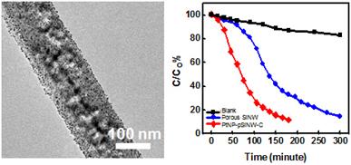
Qu, Y.; Zhong, X.; Li, Y.; Liao, L.; Huang Y. and Duan X.
(2010). Photocatalytic properties of porous silicon
nanowiures, J. Mater. Chem. 20, 3590-3594
(doi:10.1039/c0jm00493f)
 �� |
|
 |
��
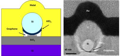
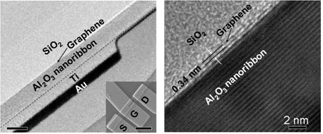
Liao, L.; Bai, J. W.; Qu, Y. Q.; Lin, Y. C.; Li, Y. J.;
Huang, Y.; and Duan X. (2010) High-k Oxide Nanoribbons as Gate
Dielectrics for High Mobility Top-gated Graphene
Transistors,
Proc. Natl. Acad. Sci.
U.S.A.
107, 6711 (doi: 10.1073/pnas.0914117107).
�� |
|
 |
��
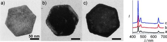
Zhang, H.; Li, Y.; Ivanov, I.A.; Qu, Q.; Huang, Y. and
Duan, X. (2010).
Plasmonic modulation of the upconversion fluorescence in
NaYF4:Yb/Tm hexaplate nanocrystals using Gold
nanoparticles or nanoshells,
Angew Chemie Intl. Ed. 49, 2865-2868
(doi: 10.1002/anie.200905805).
�� |
|
 |
��
Liao, L.; Bai, J. W.; Lin, Y. C.;
Qu,
Y. Q.;
Huang,
Y.;
and Duan,
X. (2010). High performance top-gated graphene nanoribbon
transistors using zirconium oxide nanowires as high-k gate
dielectrics, Adv. Mater. 22, 1941-1943 (doi: 10.1002/adma.200904415).
�� |
|
 |
��
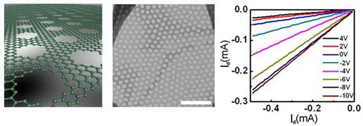
Bai, J.; Zhong, X.; Jiang, S.; Huang Y. and Duan, X.
(2010). Graphene nanomesh, Nature Nanotech.
5, 190-194.
(doi: 10.1038/nnano.2010.8).
�� |
|
 |
��
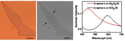
Liao, L.; Bai, J. W.; Qu, Y. Q.; Huang, Y.; and Duan, X.
(2010). Single-layer graphene on Al2O3/Si
substrate: better contrast and higher performance of
graphene transistor, Nanotechnology 21, 015705 (doi: 10.1088/0957-4484/21/1/015705).
�� |
|
YEAR 2009 AND BEFORE |
|
 |
��
Qu, Y.; Liao, L.; Li, Y.; Zhang, H.; Huang, Y. and Duan,
X. (2009). Electrically conductive and optically active
porous silicon nanowires, Nano. Lett. 9, 4539-4543
(doi: 10.1021/nl903030h)
 �� |
|
 |
��
Bai, J; Duan, X and Huang Y. (2009). Rational fabrication of
graphene nanoribbons using a nanowire etch mask, Nano.
Lett. 9, 2083-2087 (doi: 10.1021/nl900531n).
�� |
|
�� |
Duan, X.
(2009).
Nanowire thin films for flexible macroelectronics. in
Encyclopedia of Materials, Elsevier Science Ltd. |
|
�� |
Duan, X.
(2008). Nanowire thin-film transistors: a new avenue to high
performance macroelectronics, IEEE Trans. on Electron
Dev. 55, 3056-3062. |
|
�� |
Duan, X.
(2007).
Assembled semiconductor nanowire thin films for high
performance flexible macroelectronics, MRS Bull.
32, 134-142. |
|
�� |
Huang, Y.; Duan,
X.
and Lieber, C. M. (2005).
Semiconductor nanowires: nanoscale electronics and
optoelectronics, in Dekker Encyclopedia of Nanoscale
Science and Technology, J.A. Schwarz, ed.
(Marcel Dekker, Inc.). |
|
�� |
Duan, X.
and Lieber, C.M. (2005). Semiconductor nanowires: rational
synthesis, in Dekker Encyclopedia of Nanoscale Science
and Technology, J.A. Schwarz, ed. (Marcel Dekker, Inc.). |
|
�� |
Huang,
Y.; Duan X. and Lieber C. M. (2005). Semiconductor
nanowire for multi-color photonics. Small 1,
142-147. |
|
�� |
Duan, X.;
Niu, C.; Sahi, V.; Chen, J.; Parce, W.; Empedocles S. and
Goldman, J. (2003). Flexible nanowire thin film transistors.
Thin silicon newsletter 5, 4-5. |
|
�� |
Duan, X.;
Niu, C.; Sahi, V.; Chen, J.; Parce, J.W.; Empedocles, S. and
Goldman, J. (2003). High performance thin film transistors
assembled from semiconductor nanowires and nanoribbons.
Nature 425, 274-278. |
|
�� |
Duan, X.;
Huang, Y.; Cui, Y. and Lieber, C.M. (2003). Nanowires
nanoelectronics assembled from the bottom-up, in
Molecular Nanoelectronics, M.A. Reed and T. Lee, eds.
(American Scientific Publishers). |
|
�� |
Duan, X.;
Huang, Y.; Argarawal, R. and Lieber, C.M. (2003). Single
nanowire electrically driven laser. Nature 421,
241-245. |
|
�� |
Cui, Y.; Duan, X.; Huang Y. and Lieber, C.M. (2003).
Nanowires as building blocks for nanoscale science and
technology, in Nanowires and Nanobelts: Materials,
Properties and Devices, Z. L. Wang, ed. (Kluwer
Academic/Plenum Publishers). |
|
�� |
Duan, X.;
Huang,
Y. and Lieber, C.M. Nanowire nanocircuits. (2003), in
McGraw-Hill Year Book of Science and Technology, E.
Geller et al., eds. (McGraw-Hill, New York), pp.272-276. |
|
�� |
Duan, X.;
Huang, Y. and Lieber C. M. (2002).
Nonvolatile memory and programmable logic from
molecule-gated nanowires", Nano Letters, 2, 487-490.
|
|
�� |
Huang, Y.; Duan, X.; Cui, Y. and Lieber, C.M.
(2002).
Gallium nitride nanowire nanodevices. Nano Letters 2,
101-104. |
|
�� |
Huang, Y.; Duan, X.; Cui, Y.; Lauhon, L.; Kim, K. and
Lieber, C.M. (2001).
"Logic gates and computation from assembled nanowire building
blocks, Science 294, 1313-1317. co-first
author. |
|
�� |
Wang, J.; Gudiksen, M. S.; Duan, X.; Cui, Y. and
Lieber C.M. (2001).
Highly polarized photoluminescence and
polarization-sensitive photodetectors from single indium
phosphide nanowires", Science 293, 1455-1457. |
|
�� |
Li, Y.; Wang, Z.; Duan, X.; Zhang, G. and Wang, C.
(2001).
Solvothermal reduction synthesis of InSb nanocrystals��,
Adv. Mater. 13, 145-148. |
|
�� |
Huang, Y.; Duan, X.; Wei, Q. and Lieber, C. M.
(2001).
Directed assembly of one dimensional nanostructures into
functional networks��, Science 291, 630-633.
co-first author. |
|
�� |
Duan, X.;
Huang, Y.; Cui, Y.; Wang, J. and Lieber, C.M. (2001).
Indium phosphide nanowires as building blocks for nanoscale
electronic and optoelectronic devices. Nature 409,
66-69. |
|
�� |
Cui, Y.; Duan, X.; Hu, J. and Lieber, C.M. (2000).
Doping and electrical transport in silicon nanowires��, J.
Phys. Chem. B 104, 5213-5216. |
|
�� |
Duan, X.;
Wang, J. and Lieber, C. M. (2000).
Synthesis and optical properties of gallium arsenide
nanowires. Appl. Phys. Lett. 76, 1116-1118. |
|
�� |
Duan, X.
and
Lieber, C. M. (2000). General synthesis of compound
semiconductor nanowires. Adv. Mater. 12, 298-302.
|
|
�� |
Duan, X.
and
Lieber, C. M. (2000).Laser-assisted catalytic growth of
single crystal GaN nanowires. J. Am. Chem. Soc.
122, 188-189. |
|
�� |
Li, Y.; Duan, X.; Qian, Y.; Yang, L. and Liao, H.
(1999). Nanocrystalline silver particles: synthesis,
agglomeration and sputtering induced by electron beam. J.
Colloid and Interf. Sci. 209, 347-349. |
|
�� |
Li, Y.; Duan, X.; Liao, H. and Qian, Y. (1998).
Self-regulation synthesis of nanocrystalline ZnGa2O4
by hydrothermal reaction��, Chem. Mater. 10,
17-18. |
|
�� |
Li, Y.; Duan, X.; Zhang, J.; Wang, H.; Qian, Y.;
Huang, Z.; Zhou, J.; Yuan, S.; Liu, W. and Zhu, C. (1997).
Giant magnetoresistance in bulk La0.6Mg0.4MnO3.
J. Mater. Res. 12, 2648-2650. |
|
�� |
Li, Y.; Duan, X.; Qian, Y.; Yang, L.; Ji, M. and Li,
C. (1997).
Solvothermal co-reduction route to nanocrystalline
III-V semiconductor InAs. J. Am. Chem. Soc. 119,
7869-7870. |
|
�� |
Li, Y.; Li, C.; Zheng, H. and Duan, X. (1997).
Preparation and characterization of nanocrystalline NiO in
mixed solvent. Chem. J. Chinese U. 18,
1921-1923. |
SELECTED PATENTS
(out of over 50 patents/patent applications) |
|
Duan, X.
and Liu, C. (2010). Methods and devices for forming
nanostructure monolayers and devices including such
monolayers.
United States Patent 7,776,758. |
|
Duan, X., Bernatis, P.; Fischer-Colbrie, A.; Hamilton, J.M.; Lemmi,
F.; Pan, Y.; Parce, J.W.; Pereira, C.X.Y. and Stumbo, D.P.
(2010). Systems and methods for harvesting and reducing
contamination in nanowires. United States Patent
7,741,197 |
|
Duan, X.; Daniels, R.H.; Niu, C.; Sahi, V.; Hamilton, J.M. and
Romano, L.T. (2010). Methods of positioning and/or orienting
nanostructures. United States Patent 7,651,944. |
|
Duan, X.; Chow, C.Y.H.; Heald, D.L.; Niu, C.; Parce; J.W. and Stumbo,
D. (2009). Nano-enabled memory devices and anisotropic
charge carrying arrays. United States Patent
7,595,528. |
|
Duan, X.;
Niu, C. and Empedocles, S. (2008). Large area nanoenabled
macroelectronic substrate and uses therefor. United
States Patent 7,427,328. |
��
|